DE Oct 07th 2025 A Oct 09th 2025
![]() Arizona.
Arizona.
Marchés
Contrôle industriel
Gammes de produits
Imagerie par Bande Spectrale
Marques
Photonis, Xenics
Technologies
Technologie ultraviolet, Technologie dans le proche InfraRouge, Technologie infrarouge LWIR
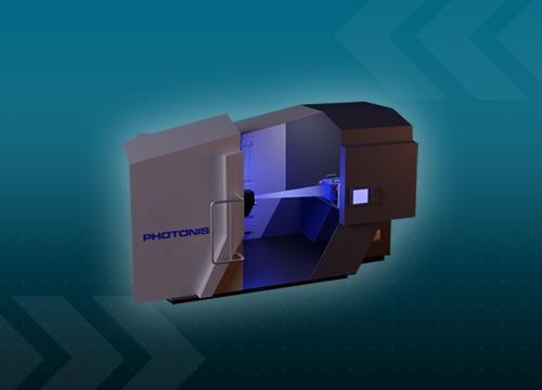
Discover the Future of Semiconductor Imaging at SEMICON West 2025
Join Exosens at Booth #2082, October 7–9 at the Phoenix Convention Center and explore how our Photonis and Xenics imaging technologies are advancing semiconductor and microelectronics innovation.
SWIR Microscopy – High-resolution imaging beyond the visible spectrum to detect sub-surface features, material defects, and wafer-level anomalies.
LWIR Thermography – Precise thermal mapping for identifying hotspots, process deviations, and equipment reliability issues in real time.
UV Dark Field Inspection – Enhanced defect detection by capturing scattered light from particles, scratches, and edge defects on wafers and photomasks.
Spanning UV to LWIR, our sensors, cores, and cameras deliver industrial-grade performance at competitive cost, helping fabs and equipment makers increase yield, reduce downtime, and accelerate throughput.
Learn more about our solutions: Ultraviolet, Visible & Infrared Imaging | Exosens
Contenu connexe

Oct 27th 2025
Résultats 9M 2025
Exosens enregistre une forte performance sur les 9M 2025, dans un marché de la Défense très dynamique
Colorado .
DE Oct 08th 2025 A Oct 09th 2025
CH4 Colorado 2025

Oct 14th 2025
Cession de parts Exosens
HLD Europe a annoncé hier avoir conclu un accord avec Theon International, principal client du groupe, pour la cession de 9,8 % du capital d’Exosens...
Oct 09th 2025
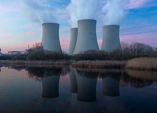
High-Temperature Detectors for Next Generation Reactors
Proven reliability up to 800°C and beyond for SMR and AMR applications. Built on the combined legacy of Photonis and Centronic—80+ years of neutron detection excellence.
Paris.
DE Nov 18th 2025 A Nov 21st 2025
Milipol Paris 2025
Join Exosens at Milipol Paris 2025, the world’s leading event for homeland security and safety, taking place at Parc des Expositions Nord Villepinte in Paris, France.
Coronado Springs Resort and Convention Center .
DE Oct 06th 2025 A Oct 09th 2025
ASNT exhibition 2025
Join Exosens at ASNT 2025 Annual Conference - Coronado Springs Resort and Convention Center – Orlando, FL Booth: #1128